Quantcast
Channel: Interfacing(USB - RS232 - I2c -ISP) Projects - PIC Microcontroller
Viewing all 320 articles
Browse latest View live

Simple mass storage for your microcontroller project

$
0
0

Do you want gigabytes of storage for your microcontroller? Would you like a simple way to tranfer files from your PC to your picaxe or arduino or other micro project?

This little projects demonstrates the uDrive that can be set up as an extra drive on a PC. Copy files to and from the SD card, then put it in the uDrive and talk to it with 5 simple commands:

Read – Read a file off the drive
Write – Write a file to the drive
Dir – get the directory listing of files on the drive
Erase – erase a file
Initialise – send 1 byte at your preferred baud rate Simple mass storage for your microcontroller project

Step 1: Connecting to your microcontroller

Connection uses 5 wires: Gnd, Power, Tx, Rx and an optional reset line. The reset line can be left unconnected if no reset is needed.

The uDrive works from 3 to 5V so can interface to a wide range of controllers.

Step 2: Copying files across

Copying involves taking the micro SD card out of the uDrive and putting it into a micro-to-standard SD adaptor. This goes into a USB adaptor that plugs into the PC and then the SD card appears as another drive on the PC. The micro SD is the small purple part seen on the left of this picture. The USB to SD adaptor cost $5 including shipping on ebay. Most micro SD cards come with micro to standard adaptors and the total cost of the package is under $10 for gigabytes of storage.

Step 3: Accessing the files from a microcontroller

Microcontrollers all have different languages; assembly, C, Basic, Spin etc. You will have to write your own exact code, but below is an example using vb.net. This is still a bit complicated, but it is a lot easier than trying to talk to a SD card using bit-bang SPI code.

For the purposes of testing, we have built a little uDrive to RS232 converter. We are actually talking back to a PC via the PC serial port (or via a USB to serial adaptor), which seems a bit pointless, but it at least enables the device to be tested quickly and code debugged.

The Max232 converts the 0V/5V levels from the uDrive into valid RS232 voltage levels. Simple mass storage for your microcontroller project schematic

Step 4: Testing using 4dsystems’ software

The first test is to run some testing software from 4dsystems http://www.4dsystems.com.au/prod.php?id=22

This has pre-written test routines that not only check the device is working, but also indicate the bytes going back and forth. This makes it much easier to work out how to write your own code.

You can also talk to the card in raw mode, but using DOS mode that a PC can understand is a lot simpler. A file can be tiny – just 1 byte if you wish.

For more detail: Simple mass storage for your microcontroller project

The post Simple mass storage for your microcontroller project appeared first on PIC Microcontroller.


RS232 – Infra-Red Interface

$
0
0

Description

This project is a Microchip PIC microcontroller with an RS232 serial interface on one side and an Infra-Red receive and transmit interface on the other.

Important – All mention of RS232 on this page actually refers to RS232 waveforms operating at 5V TTL levels not +/-12V levels which would destroy the PIC device. An appropriate converter between the two must be used.RS232 - Infra-Red Interface

By sending commands on the RS232 interface it is possible to receive or transmit a sequence of bits modulated as a series of on/off states in a 38 kHz infra-red carrier signal. Infra-Red remote controls use a carrier signal (typically around 38 kHz) so that there is no confusion with sunlight etc. The carrier is turned on and off to represent the bit sequences at a lower rate, for example 500 Hz).

Either a raw sequence of on/off states can be captured or transmitted or one of a predefined set of remote control formats can be emulated (receive or transmit).

The circuit is built on stripboard with a DIL packaged IC and conventional through-hole passive components. The PCB is glued into the base of a small box for convenience.

The PIC microcontroller is the only IC and mounted approximately in the centre of the PCB. The RS232 connector is on the right with the Infra-Red receiver and LED for transmit on the top. Rather than use a photo-diode and decoding the signal a complete module (in this case a TSOP1738 photo module) is used. This contains all of the circuitry to detect a signal with a carrier frequency of 38 kHz.

PIC Software

The PIC software is written in assembler and this project was the development platform for the Infra-Red library functions.

The complete information for this project is available for download. This includes the library functions for the RS232 and IR interfaces as well as the circuit diagram, layout diagram and various C programs. This project is included in the library of PIC code that is available for download.RS232 - Infra-Red Interface schematic.jpg

The circuit diagram is quite simple with the RS232 interface (a connector), PIC (IC and decoupling capacitor) and ICSP (socket, 1 diode and 1 resistor). For the Infra-Red part it is more complicated. There is a transistor (operating as a switch) and a capacitor to ensure that sufficient current can be switched to drive the LED. Driving the LED with the PIC alone would not allow enough current to transmit a strong Infra-Red signal. There is also a small red LED to show when the Infra-Red one is operating.

This simple PCB layout diagram shows the placement of the components on the stripboard. The view is from the top of the PCB, the same as in the photograph.


For more detail: RS232 – Infra-Red Interface

The post RS232 – Infra-Red Interface appeared first on PIC Microcontroller.

USB Reprogrammable iButton door lock

$
0
0

iButtons are small button like casings that communicate with only 2 wires. They are incredibly robust and all have a unique serial number which is hardware written into the device and never repeated. They are cheap (about 1 Pound / 1,50 Euro/ $2)

This serial number allows the keys to be truly unique and thus are effectively secure. I have seen them used:
>as the till logon device at bars
>in securicor money cases
>computer logins
>as secure dongles used with expensive software.
>…as door locks!

The problem with using them for the beginner, is that you have to be able to program hardware to read them and if you loose the key, the locking device is useless!

This Instructable shows you how to build a lock, and a USB programmer that enables you to write new keys to the lock in seconds, without dismantling the unit. Making the lock completely secure and updatable for up to 80 keys at a time. The lock can work on between 5-30V AC or DC and so is incredibly flexible; designed to work on the same voltage as your electronic door release – you can buy the cheapest or most expensive one you find, Fail-Locked or Fail-Unlocked, AC or DC, 12V or 24V.USB Reprogrammable iButton door lock

What you will need:
>Components (see next)
>PIC programmer
>Electronic door release.
>PCB making equipment (if you want to make it look puurdy)

NOTE!!!
This is an old instructable that I haven’t uploaded for some reason. If you have trouble building it, email me and I will happily help – however, I can’t guarantee I’ve made it as simple as possible – sorry – hopefully it’ll give inspiration if nothing else.

Step 1: The Process

Firstly you’ll need to decide which type of lock you need.

FAIL SAFE/UNLOCKED remain open when the unit looses power. This would generally be used if the door nbeeds to be accessable in the event of a power failure – e.g Fire

FAIL SECURE/LOCKED remain locked unless power is applied to the lock. These would be more appropriate when using a traditional door entry system, having the door traditionally locked at all times, unless power is applied.

Below is a flow chart to show how the device operates.
Simply, if you enter a key, the microprocessor firsts checks to see if it’s a programming key, or it’s an access key.

If it’s an [iButton] access key, the microprocessor checks against the list of known keys stored in it’s EEPROM (memory), if it finds it, it lets you in. Otherwise it will send a red-light to say that no access is granted.

If it’s a reprogrammable key of any type (e.g. an iButton with a new list of keys to store on the internal EEPROM). It will check if the ibutton is allowed to re-program the internal EEPROM but checking it’s authentication code. (This is programmed into the iButton by the USB programmer and this you can’t change – see last page for info).
If the iButton is allowed to program the internal EEPROM, the LED will flash Green/Orange and then microprocessor will pull all the key-codes off the iButton and store them to it’s internal EEPROM. This will cause the LED to flicker and could take up to 20 seconds – do not remove the key while this is happening. The LEDS will then pulse green to indicate the programming is over – now remove the iButton.

Step 2: The components

OK so the instructable is pretty easy, i give you the schematic, parts list, hex file, and you build it – simple!
I’m going to give the parts list and the Rapid Electronics ( http://www.rapidonline.com ) part number so you can source your own supplier – although rapid is pretty good!
Heres the parts listDoor Lock

1x Bridge Rectifier (rapid# 47-3202)
1x 5v 7805 voltage regulator (rapid# 47-3313)
1x SIL relay (rapid# 60-0670)
1x 100uf cap (rapid# 10-3260)
1x 470uf cap (rapid# 11-0275)
1x 220f cap (rapid# 11-0260)
2x 1k resistor
1x 4k7 resistor
1x 16f628 PIC micro
1x 24LC04 4k eeprom (rapid# 22-0170)
1x 8pin dil holder
1x 18pin dil holder
1x DPDT mini switch (rapid# 76-0220)
1x 3pin header (rapid# 22-0515)
1x jumper (rapid# 77-0237)
2x 2pin terminal block (rapid# 21-1700)
1x Electronic release ( http://www.directlocks.co.uk )
1x iButton probe with BiColour LED (MBL)(part# hc00039 http://www.homechip.com )
1-80x DS1990A iButtons ( http://www.homechip.com )

The USB programmer

1x 18f2550 PIC micro
1x 20MHz XTAL
2x 22pf caps (ceramic disc)
1x 220nf cap
1x 1k res
1x LED (any colour)
1x USB B-socket
1x iButton holder probe DS1402 (any will do) ( http://www.homechip.com )
1x DS1973 iButton ( http://www.homechip.com )

Some of the iButton hardware or buttons may be obtained free by ordering samples from http://www.ibutton.com (direct from maxim).USB Reprogrammable iButton door lock schematic

Step 3: Schematic and PCB for lock

Below is the schematic, the PCB and the final example photo of the lock. For a printable PCB layout, see downloads.
For a high res version of the Schematic, click the i and download the file (14kb).

PCB layouts are available on the download page.

Step 4: Schematic, PCB and photo of the programmer

below is the schematic, example PCB and photo of the final produced PCB of the USB programmer

The post USB Reprogrammable iButton door lock appeared first on PIC Microcontroller.

Computer-Controlled Light-Up Water Fountain using pic-microcontroller

$
0
0

System Overview

La Fontaine Du Campus Est (The Fountain of East Campus) is a computer-controlled, servo-actuated, LED and halogen-lit, sump-pump powered water fountain. It features five streams of water that can each be individually controlled (on/off) as well as pivoted (90 degrees of freedom). Each stream of water is lit by a halogen light. The perimeter of the fountain has RGB triplets that can perform various animations. The fountain and water are also illuminated by eight Luxeon LEDs. The entire system is controlled by a PC that sequences through a choreographed file called a ShowFile. Three circuit boards act as an interface between the fountain and the computer: a valve control board, an LED control board, and a servo control board. All but the last were custom built for La Fontaine Du Campus Est.

Computer-Controlled Light-Up Water Fountain

The above diagram shows the connections between the three circuit boards that run the fountain devices, the Fountain Director PC, and the fountain hardware itself.

The underside of the fountain. Blue objects with attached hoses are the washing machine solenoids used to switch each nozzle on and off.

Fountain-side electronics are mounted in a sealed box under the fountain surface.

Valve/Halogen Controller

The valves to turn the nozzles on or off are activated by relays. The halogen lamps that point up the water streams are also activated by relays. The valve/halogen controller board is a custom circuit that interfaces via USB and activates these inductive loads on demand. There is also built-in logic that ensures a relief valve is always in the proper state of operation. The circuit is based around a PIC 18-series microcontroller and an FTDI USB-UART converter.

Downloadable valve/halogen controller source code:

Valve/Halogen Controller Source

Computer-Controlled Light-Up Water Fountain

LED Controller

The LED controller is designed to serve as a general purpose lighting controller. It controls the 24 fountain-mounted LEDs as well as the eight Luxeons. All lighting animations are built into the onboard memory. A computer interfaces with the board and tells it which animation to play, and with what color(s).


For more detail: Computer-Controlled Light-Up Water Fountain

The post Computer-Controlled Light-Up Water Fountain using pic-microcontroller appeared first on PIC Microcontroller.

USB digital GPIO I/O extender using pic microcontoller

$
0
0

description

Add general purpose input/output lines to your computer based projects. This circuit is a 12 pin digital GPIO interface using the Microchip PIC18f14k50 microcontroller which connects to an USB host port. The microcontroller is available in through-hole DIP20 and SMD packages, too.

Circuit diagram

The device is powered by the USB bus. 12 port bits can be set on a bit-by-bit basis to input or output direction. All LEDs on the schematic are optional, and are only shown for testing the device. You can find the USB connector pinouts at http://pinouts.ws/usb-pinout.html

USB digital GPIO I O extender

Controlling the GPIO interface

A computer, any OpenWrt router, Raspberry Pi or other Linux development board with an USB host port can be used to control the GPIO extender. The “controlio” utility runs on all platforms.

Usage: controlio [options] <command> [value]
Control an USB I/O port

 -d, --device <vendorid>[:productid]
    Select only device(s) with USB vendorid[:productid], default=0x04d8:0xf7c0
 -s, --serial <serial number>
    Select only the device with the given serial number, default=any
 -o, --output <base>
    Set output format. Base x=hexadecimal (16), b=binary (2), d=decimal (10), default=x
 -v, --verbose
    Verbose mode
 -V, --version
    Show program version
 -h, --help
    Show usage and help

The commands are:

command line description
controlio getport read the digital I/O port states
controlio setdir <n> set the digital I/O port directions. Use bit 1 to set direction to input, bit 0 to set direction to output
<n> is a 16-bit number
controlio setport <n> set the digital I/O port output states. Sets all output I/O pins. Use bit value of 1 to set output to HIGH, 0 to set output to LOW
<n> is a 16-bit number
controlio setbit <n> set the selected digital I/O port output pins to HIGH. Use bit value of 1 to select I/O pins to set
<n> is a 16-bit number
controlio clearbit <n> set the selected digital I/O port output pins to LOW. Use bit value of 1 to select I/O pins to clear
<n> is a 16-bit number

Numbers for <vendorid>, <productid> and <n> can be given in decimal, hexadecimal or binary format. Hexadecimal numbers are prefixed with ‘0x’, binary numbers are prefixed with ‘0b’. Command output base can be also set to hexadecimal with switch -ox, decimalwith switch -od or binary with switch -ob.

Mapping of I/O port pins, directions to parameter <n> and buffer output:

controlio getport output buffer[0] buffer[1]
I/O pin RC7 RC6 RC5 RC4 RC3 RC2 RC1 RC0 RB7 RB6 RB5 RB4
controlio setport <n>
controlio setdir <n>
controlio setbit <n>
controlio clearbit <n>
bit#7 bit#6 bit#5 bit#4 bit#3 bit#2 bit#1 bit#0 bit#15 bit#14 bit#13 bit#12 bit#11 bit#10 bit#9 bit#8

Examples:

command line example explanation
controlio setdir 0xffff set all I/O pins as input
controlio getport Read the digital I/O port states. The output is 16 bits long, and is shown in the selected base (use the -o command line switch). Output ports usually read back the state they are set to. Input ports read their externally set state.
Command output is:
0xf0ff
controlio -od getport Read the digital I/O port states. Same as the previous command, but the output is printed in decimal:
61695
controlio -ob getport Read the digital I/O port states. Same as the previous command, but the output is printed in binary:
0b1111000011111111
controlio setdir 0 set all I/O pins as output
controlio setport 0 set all output I/O pins LOW
controlio setport 12 or
controlio setport 0xc or
controlio setport 0xb1100
set the RC2 and RC3 I/O pins HIGH,  other output pins LOW (works only on output pins)
controlio setbit 32768 or
controlio setbit 0x8000 or
controlio setbit  0b1000000000000000
set the RB7 output pin HIGH, don’t change other output pins (works only if RB7 is an output pin)
controlio clearbit 4097 or
controlio clearbit 0x1001 or
controlio clearbit 0b1000000000001
set the RB4 and the RC0 output pins LOW, don’t change other output pins (works only if RB4 and RC0 are output pins)

Download

Download the full package. Contents:

bin/device_firmware the firmware HEX file for the PIC18F14K50 device
bin/host/linux.x86 the Linux controlio utility executable
bin/host/openwrt the OpenWrt packages for the controlio utility
bin/host/raspberry Raspberry Pi binaries for the controlio utility
bin/host/win.x86/driver the drivers for using the GPIO device under Windows
bin/host/win.x86 the Windows controlio.exe utility
src/device_firmware the C18 source code for the PIC18F14K50 firmware
src/host/openwrt the source code for building the OpenWrt package
src/host/posix the source code for building the controlio utility for Linux and other POSIX compatible systems
src/host/python example code for accessing the GPIO device from python

Previous, obsoleted version with assembly firmware

Installing on the PIC18F14K50 device

Program the bin/device_firmware/usbio.hex file with a Microchip Pickit 2 or Pickit 3 programmer into the chip.

USB digital GPIO I O extender

Installing on the host

Linux

  1. install libusb-0.1 with “apt-get install libusb-0.1” or “yum install libusb”
  2. copy bin/host/linux.x86/99-usbio.rules to /etc/udev/rules.d/ – this lets everyone use the device
  3. copy bin/host/linux.x86/controlio to the host
  4. connect the GPIO extender to the USB port

Raspberry Pi

  1. install libusb-0.1 with “apt-get install libusb” on Raspbian or “yum install libusb” on Pidora
  2. copy bin/host/linux.x86/99-usbio.rules to /etc/udev/rules.d/ – this lets everyone use the device
  3. copy bin/host/raspberry/controlio to the host
  4. connect the GPIO extender to the USB port


For more detail: USB digital GPIO I/O extender

The post USB digital GPIO I/O extender using pic microcontoller appeared first on PIC Microcontroller.

OSOMCOM POCSAG BTS using pic microcontoller

$
0
0

The BTS or Base Transmitter Station is the device that transmit the POCSAG messages to the pager. It is the radio interface of the POCSAG network.

THE HARDWARE

The current version of the BTS hardware is a small board with a pic 18F microcontroller with a firmware that receive commands through an UART/RS232 port, create the POCSAG message and transmit it using the ADF7012 UHF transmitter.

This board has not be designed to be used exclusively with OSOMCOM POCSAG but to be used as a generic low power radio transmitter. Other uses of this board include experimenting with 433MHz keyboards, car/garage remotes, data links, APRS, etc.

The board has been designed to be very cheap (less than 15$) and easy to develop with.

OSOMCOM POCSAG BTSBoard features

  • CPU: PIC 18F14K22 @ 16MHz
  • Memory: 16KB Flash / 512 Bytes RAM / 256 EEPROM
  • Transmission frequency: selectable from 75MHz to 1GHZ (but some parts values may need to be changed. More about this later)
  • Supported modulations: FSK/GFSK/OOK/GOOK/ASK. (FSK is used for POCSAG)
  • Transmission bitrate: selectable up to 179.2 kbps (512/1200/2400 for POCSAG)
  • Transmission power: selectable up to 14 dBm (20mW)
  • UART/RS232 port
  • Debugging/programming port for ICD/PICKIT
  • Expansion port with 4 GPIOs
  • SMA connector for antenna
  • Power: 3.3 volts ; ~50mA
  • Size: 4.4 cm x 4.6 cm

Power supply

The power supply has a very simple and standard design.

The 5 volts input is transformed to a 3.3 volts supply using  the MCP1700T-3302 low-drop voltage regulator from Microchip. C1, C2 and C3 filter the input and output power.

A diode protecting the input from a reversed connection could be handy, but I didnt put it in the design. I am just confident that the user is not that stupid…

– Microcontroller

The brain of the board is a Microchip PIC 18F14K22.

– The radio module

A ADF7012 from Analog Devices is used as radio module.

This handy UHF low-power radio transmissor supports FSK, GFSK, OOK, GOOK and ASK modulation at a maximum rate of 179.2 kbps and the integrated Power Amplifier can deliver up to 20 mW without using an external antenna driver.
An internal PLL with selectable divisor synthesize almost any desired output frequency in a range from 75MHz to 1GHZ using just a 4MHz quartz.

A SPI interface is used to configure the transmisor. Modulation scheme, output power, output frequency and  other transmission parameters are selectable through this interface.

In my opinion, due its versatility, flexibility and simplicity to use, this is one of the best sub-GHz integrated transmisor out there. However, the lack of documentation and examples make it a little bit frustrating to work when you are starting. The datasheet is sometime confusing and sometimes insufficient. For example, it doesn’t give a table or graph with the output impedance of the RF output. HOW THE HELL ARE YOU GOING TO MATCH THE ANTENNA IF YOU DONT KNOW THE IMPEDANCE? Of course… you can always use a network analyzer and measure it, but unfortunately I don’t have access to one, so I just did my best trying to guess the impedance at my working frequency using the schematics of the application examples. They are for different frequencies, but I did an interpolation and… it works more or less fine.

I don’t want to make a deep explanation of the design process and inner working of the radio module, but I will make a brief description of the function of the different parts. If you need more information, refer to the ADF7012 datasheet.

The Q1 4MHz crystal define the output frequency.
To be more exact, the crystal frequency defines the output frequency  resolution. The output frequency is a defined with the  equation

Fout = Fcrystal · (N/R)  · OD

being N a 8+12 bits fractional number, R a 4 bits integer number and OD (Output Divider)  is 1,2,4 or 8. The value of N,R and OD are selectable through the SPI interface.
In theory, almost any output frequency is selectable with almost any input frequency, but choosing a lower frequency crystal gives you more resolution and introduces less spurious noise.

In case we use FSK or GFSK, the crystal frequency also defines the frequency deviation resolution:

Fdeviation = (Fcrystal / R)  · (M / 4096)

M (Modulation Number) is a software selectable 9 bits integer number.

The L1 coil controls the VCO frequency. The value of the coil has to be chosen according to the desired output frequency. The current value of 8.7 nH is appropiate to work in the frequency ranges of 70-77.5 MHz, 140-155MHz , 280-310 MHz and 560-620MHz. If you would like to personalize the circuit to make it work in a different frequency, you have to refer to the datasheet graph and choose an appropiate inductance value.

The Loop Filter formed with C10, C11, C12, C13, C14, C15, R4, R5 and R6 filters the VCO tunning voltage. In practice, the bandwith of this filter limits the maximum transmision datarate. When using FSK, the bandwith of this filter should be  three times the bandwith of the data rate.

The easiest way to calculate the values of the filter is using the “ADI SRD Design Studio” software availabe for free in the Analog Device website.
For our current needs, a 30KHz filter bandwith has been implemented.

The antenna matching network

As commented before, the RF output impedance of the ADF7012 at 150MHz is an unknow, so the antenna matching is not easy without the proper resources.

I don’t have a network analyzer to measure the output impedance so I did some guess and some try-and-error process. The result is not perfectly matches but is good enough as the transmisor signal range is more or less the expected for a 20 mW emission.

Be aware that L4, L6 and L8 are unpopulated. I put those coil footprints in the PCB just in case a fine tuning is required by adding another coil or capacitor in parallel.

If you need to modify the BTS schematic to transmit in a different frequency than 140-160MHz, you have to change this antenna matching network to adapt it to your needs.
If you want to work with 315, 433, 868 or 915 MHz, you can use the matching network recommend in the datasheet.

– I/Os and connectors

S1 is a push-button that can be used to launch in the firmware some tasks.

SV1 is a RS232 connector to communicate with the BSC or a host computer.  It uses 3.3v signals but is tolerant to 5v. You can use a RS232 TTL – USB bridge to connect the BTS to your computer BSC system.

SV2 is a General Purpouse I/O port. It has 4 free GPIOs that can be connected to any sensor or system. GP1 is also an analog input, so an analog sensor like a temperature sensor can be connected.

SV3 is the ICD debug port. The microcontroller can be programmed or debugged with an ICD, PICKIT or similar device.

THE FIRMWARE

The last version of the firmware can be downloaded here.

The firmware has been written in C using the MPLAB X IDE and the XC8 compiler in free mode. It is important to compile it using the version 1.20 or superior of the XC8. Earlier versions dont optimize the code and the binary will not fit into the microcontroller.

The main function of the firmware is to transmit POCSAG encoded messages. However, in the firmware source there is a complete library to configure and control the ADF7012 radio module, so it would be easy to modify the firmware to transmit using other digital protocols.

USAGE AND COMMANDS

The best way to use the POCSAG BTS  is connecting it to a device or computer running the Osomcom POCSAG BSC software and let the BSC to control the BTS. However, if you need something simple you can just connect the BTS to your computer’s RS232 port  using a USB-RS232 converter and use a terminal program to send commands to the BTS. The current firmware puts in the RS232 port a command console  that can be used to configure the BTS and send messages.

The configuration of the RS232 is 9600 Bauds 8-N-1.

The current available commands are:

– SEND (A|N|I) RIC MESSAGE:

Send a POCSAG message to the specified RIC. The first parameter indicates if the message has to be send like an Alphanumeric message, a Numeric message or an Idle message.

An hexadecimal representation of the sent batches is printed.

– CONFIG [PARAM] [VALUE]:

The config command without arguments  prints a list of the configurable parameters and their current value. To set a new value, send the parameter name and the new value with the CONFIG command.

This is the list of the available parameters:

  • FREQ: Frequency in Herzs. If you set a frequency that is not reacheable by the BTS hardware, it will complaint with a ‘Init error’ message when it start to transmit (SEND, START_MS or TEST command).
  • DEVIATION: FSK deviation in Herzs. In POCSAG, the most common value is 4500.
  • BAUDS: 512, 1200 or 2400.
  • POWER: The RF output power. The value is in the range between 0 (-20dBm) and 32 (13dBm).
  • MS_SAVE_FREQ: Number of RICs between status saving when doing a ‘Mass Send’ (more info below)
  • MS_DELAY: wait time in milliseconds between the transmision of two batches of 8 messages when doing a ‘Mass Send’.

– SAVECFG:

Saves the current config in the EEPROM. The configuration is restored when the board is powered.

– LOADCFG:

Restores the config stored in the EEPROM.

– START_MS START_RIC STOP_RIC:

Start a ‘Mass Send’. It sends a message with a single ‘A’ character to all the RICs between the START_RIC and STOP_RIC. It is useful to scan RICs, when you don’t know the RIC of your pager.

8 messages for 8 consecutives RICs are packed and transmited in a single POCSAG Batch. Between two batches, some time defined by the MS_DELAY config parameter is waited.
Every MS_SAVE_FREQ number of RICs scanned, the current status of the Mass Send is stored in the EEPROM. In case the power supply is disrupted, the firmware will automatically continue with the Mass Send from the last saved status.

STOP_MS:

Stops the Mass Sending.

– RESUME_MS:

Continue with the stopped Mass Sending.

– STATUS_MS:

Shows the current state of the Mass Send (current RIC and stop RIC)

– TEST [0|1|2]:

Transmits a continous test signal with the selected pattern: ’000000…’ (TEST 0), ’111111…’ (TEST 1) or ’101010…’ (TEST 2).

I use this function to know if the ADF7012 is transmiting at the desired frequency and deviation.

– STOP_TEST:

Stops the transmition of the TEST signal.

OSOMCOM POCSAG BTS

TROUBLESHOOTING

If you have problems making the BTS to work, check the next things:

– Is every thing correctly connected/soldered? Double check the soldered parts. Are them the correct parts?

– Is the microcontroller programed?

– Is the board being powered with a 5 volts power supply? Anything between 3.7 and 6 volts should be OK.
You can know if the board is being correctly powered because one led will be light.

– Connect the BTS board to your computer using a USB-RS232 board. Open a terminal program and set it to 9600 bauds, 8-N-1. Power the board and you will see a welcome message (‘Osomcom POCSAG 0.3′). If you send any string, the board will respond with a help menu.

If you can’t make work the RS232 shell, you probably have a problem with the microcontroller. If you can get the shell but you can’t transmit anything, the problem is probably in the radio module.

– Check if there is any transmission. The best and cheapest way to do this is using an RTL-SDR dongle. I use it like an spectrum analyzer.
Open the command shell, configure the desired frequency and deviation and use the TEST 2 command to generate a test pattern signal.

If it says ‘Init Error’, the BTS can’t reach the configured frequency. Choose another frequency or if you are interested in transmitting in that one, modify the schematics (the VCO coil and the antenna matching) as suggested in the Hardware section.


For more detail: OSOMCOM POCSAG BTS

The post OSOMCOM POCSAG BTS using pic microcontoller appeared first on PIC Microcontroller.

Updated PIC 18F4550 USB Demo Board Video

$
0
0

In this video we step through a an updated version of the USB demo board. Changes include:
-circuit board will only contain bare minimum parts to demonstrate USB communication from host to device and device to host
-for both firmware and host software, we will make the projects from scratch, import downloaded USB function libraries, write main program step by step
-these changes should make it much easier for somebody new to USB communication or new to USB communication with the 18F4550 to get started
-follow along and make your own!


The post Updated PIC 18F4550 USB Demo Board Video appeared first on PIC Microcontroller.

2-Wire Keypad Interface Using a 555 Timer using pic microcontoller

$
0
0

Keypads are a very commonly used input device in microcontroller-based systems. In a keypad, multiple switches are arranged in rows and columns so that they could be interfaced to a microcontroller with a minimum number of I/O pins. For example, a 12-key keypad is arranged in a 4×3 format, which allows to interface the 12 keys to a microcontroller with only 7 connections. The location of each key on the keypad is defined by two coordinates: the row and the column. When a key is pressed, it connects its row with its column. The microcontroller must scan all the rows and columns to find out which key has been pressed. This is the most common way of interfacing a keypad to a microcontroller. There are tons of resources on the internet regarding this technique and so I am not going to discuss it here.

2-Wire Keypad Interface Using a 555 TimerToday, I am going to share with you about a new keypad interfacing technique that uses only two I/O pins of a microcontroller: one for signalling the microcontroller when a key is pressed, and the other is to read the key information. It is based on a 555 timer IC which is configured as an astable multivibrator. I am not sure if anybody has ever tried using a 555 IC for keypad interfacing, but this technique really works. I am going to demonstrate this with a 4×3 keypad (a standard telephone dial pad). A PIC16F628A microcontroller will read the output of a 555 timer IC, determine what key has been pressed, and display it on a character LCD module.

Theory

This technique is based on a very simple principle. The output frequency of a 555 astable multivibrator is defined by two resistors and a capacitor, as shown below.

If we fix R1 and C, the frequency can be varied by varying R2. In this technique, each key on the keypad connects a different R2 resistor when it is pressed, and therefore, generates a different output frequency. The microcontroller can then read the output frequency and determine which key was pressed. At first it does seem more complex as it may require floating point math regarding the frequency calculations. Besides, the frequency may not be precisely stable all the time. But this can be simplified with the proper selection of resistors and the use of the timer module inside the microcontroller. So here’s how it works:

When a key is pressed, a certain value of R2 resistor is connected between pins 7 (Discharge) and 6 (Threshold) of the 555 timer, completing the astable multivibrator circuit. The output pulses are counted for 100 ms through a timer module (used as counter) in the microcontroller. The microcontroller determines the pressed key from the number of times the timer has overflown. If the timer module overflows 5 times, the pressed key is 5. Similarly, if 0 key is pressed, the timer doesn’t overflow in the 100 ms window. Isn’t it simple now?

2-Wire Keypad Interface Using a 555 TimerCircuit diagram

The figure below shows how the 12 keys are connected to the 555 timer IC to generate 12 different frequencies. R0 through R# are 12 different resistors corresponding to those frequencies. You can see when a key is pressed, the corresponding resistor is connected between pins 6 (Threshold) and 7 (Discharge) and the astable multivibrator circuit is completed.

The values of R1 and C are 1 K and 0.01 uF. The following table shows the different values of R2 for each keys, the corresponding frequencies, and the number of times the Timer0 module overflows. Some of these resistors are made from combining two resistors together.


The post 2-Wire Keypad Interface Using a 555 Timer using pic microcontoller appeared first on PIC Microcontroller.


Joshua Marchi’s Lab Notebook using pic microcontoller

$
0
0

Week 01

January 11, 2012 (1 hour):
Met with professor Talavage to discuss the basic functionality of the headset sensor devices that will be used to collect data for this project. Discussed challenges of interfacing these devices to the base station using the USB protocol standard.

January 11, 2012 (1 hour):
Met as a team to complete preliminary project proposal.

January 12, 2012 (3 hours):
Researched USB protocol standards. Determined that the base station must have some sort of USB host to communicate with the USB sensor devices. Discovered that it would be much easier to implement USB communcation protocol with a motherboard rather than a bare microcontroller.

WEEK 01 SUMMARY
Accomplishments: Submitted preliminary project proposal. Gained insight into USB protocol standard, and determined a motherboard would be ideal to handle USB communication.
Weekly Work Total: 5 hours
Project Work Total: 5 hours

Week 02

January 18, 2012 (1 hour):
Met with Professor Vijay Raghunathan to further discuss project idea. Professor Raghunathan suggested using a BeagleBoard running embedded Linux as primary means of USB communication. The BeagleBoard would also be able to interface to a hard disk, maintaining the file system necessary to hold data obtained from several headset sensor devices.

January 18, 2012 (3 hours):
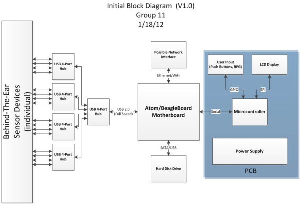
Met as a team to discuss PSSC’s for this project as well as system design. The current plan is to cascade powered USB hubs to support up to 16 USB headset sensors, which will connect to a USB port on either a BeagleBoard or Atom board. This board would also manage a file system on a hard drive disk used to store data from the headsets. A standalone microcontroller would be used control an LCD display, as well as power some LEDs and interface with the user through pushbuttons and a rotary pulse generator. The standalone microcontroller would communicate with the motherboard through a serial interface. Also, it was decided that the group would utilize Trello as a free project management service for this semester.

PSSCs:
1. An ability to obtain raw data from sensors via a USB interface with motherboard
2. An ability to store raw data and manage files on mass storage device
3. An ability to charge and monitor sensor battery status and convey to the user
4. An ability to receive user input and interface to the user through graphical display
5. An ability to communicate to the motherboard via the microprocessor using serial interface

Joshua Marchi's Lab NotebookJanuary 18, 2012 (1 hour):
Completed preliminary system block diagram (V1.0)

January 20, 2012 (1 hour):
Met with Professor Johnson to discuss concerns related to the proposed design meeting 477 course requirements. Johnson expressed that he thought the project placed too much functionality on the motherboard, leaving little functionality for the custom PCB. It was concluded that either a much larger portion of responsibility would need to moved from the motherboard to PCB, or a new project idea would need to be developed.

January 20, 2012 (2 hours):
Met with George Hadley to discuss the possibility of moving USB host functionality from the motherboard to the PCB. George felt that amount of work required to achieve this would be much too great to fully complete the design by the end of the semester. The team concluded that a new project idea would be a much better idea than trying to modify the original idea. It was concluded that the new design would be a “Reverse Geocache” device, where instead of locating a box using gps coordinates, there would be a box that would remain locked until it had been brought to the correct sequence of GPS locations.

January 21, 2012 (4 hours):
Met as a team to discuss theory of operation for the new project idea. It was determine that the newly named “RevGeo” Reverse Geocache would receive GPS signals to determine its current location, direct its user to the next “checkpoint” by the use of LEDs and a compass with tilt compensation, and unlock itself with either a solenoid or servo controlled locking mechanism when the box has reached its final destination. The box will also have an LCD screen to interface with the user, read instructions from a microSD card, and a speaker to play audio when the box unlocks. Finally an RFID “master key” system will be implemented to override the system and unlock the box at any time. A new preliminary system diagram was also developed during this meeting.

New PSSCs:
1. An ability to obtain and decode global positioning data via GPS
2. An ability to decode acceleration and magnetometer data to determine a compass heading
3. An ability to access and interpret files located on a microSD card
4. An ability to display information to the user via an LCD display
5. An ability to identify an RFID tag using an RFID reader and serial interface

WEEK 02 SUMMARY
Accomplishments: Project proposal, block diagram, and PSSCs created for initial idea, then revised to reflect new project idea.
Weekly Work Total: 12 hours
Project Work Total: 17 hours

Week 03

January 23, 2012 (3 hours):
Worked through Sparkfun Eagle tutorials for Schematic, Layout, and Custom Component Generation. Based off the knowledge gained in these tutorials, the group created a custom component for the National Semiconductor LM2675M-5 switch mode voltage regulator chip. Using this custom component, a layout and schematic was individually begun for the 5V regulator circuit described in the PADS tutorial.

January 23, 2012 (2 hours):
The group discussed a preliminary list of major components needed for the project. Items on this list are as follows: Microcontroller, GPS receiver, compass, RFID receiver, MicroSD card, locking mechanism, rechargable battery, LCD screen, speaker, case. Began more in-depth research on some of these parts, with the goal of purchasing many of these parts in the next few days.

January 24, 2012 (1 hour):
Completed the schematic and layout for the 5V regulator circuit described in the PADS tutorial, and was checked off by the George Hadley for completion of HW #2.

January 24, 2012 (1 hour):
Met as a group to finalize the TCSP presentation slides for tomorrow, and determined who would discuss each topic during the presentation.

January 25, 2012 (2 hours):
Met as a group to develop a preliminary cost sheet based on the components be used for the project. The total estimated cost for the design will be around $300. Several parts were ordered during this meeting, which will arrive by Monday of next week at the latest. Those components are as follows:

* GPS Receiver – Copernicus II DIP Module (Sparkfun)
* Tilt Compensated Compass (with breakout board) – LSM303DLH (Sparkfun)
* RFID Starter Kit (RFID module, USB reader, RFID cards) – ID-12 (Sparkfun)
* Speaker – 8ohm, 0.5W (Sparkfun)
* Pelican Case 1150 – 8.18″ x 5.68″ x 3.62″ (Amazon)

WEEK 03 SUMMARY
Accomplishments: Completed Sparkfun Eagle Tutorials as well as HW#2, preliminary parts list completed and several components purchased.
Weekly Work Total: 9 hours
Project Work Total: 26 hours

Week 04

January 30, 2012 (2 hours):
Researched microcontroller choices for this project. The PIC microcontrollers from Microchip look to be a good choice, as Microchip has a Memory Disk Drive File System library that allows for easy interfacing with SD cards. Some other requirements for a suitable microcontroller include having 4+ UART channels, 2+ I2C channels, 2+ SPI channels, and enough code and data memory for the Memory Disk Drive File System library along with all application code. Taking all of this into consideration, the PIC24FJ128GA306 looks to be a strong contender in the choice of micro for this project.

January 31, 2012 (4 hours):
Created and finalized TCSP Powerpoint on Design Contraint Analysis to be presented in class tomorrow. The microcontroller decided on for this project is the PIC24FJ256GA106, which has 256KB Flash and 16KB RAM, which will allow plenty of space for application code, as well as for the Memory Disk Drive File System Library from Microchip to assist with MicroSD interfacing. Also, the PIC24FJ256GA106 has 4 UART, 3 SPI, and 3 I2C, which satisfies the project design contraints of requiring 3 UART (GPS, RFID, PC Debug), 1 SPI (MicroSD), and 1 I2C (Digital Compass). The team decided to incorportate an FT232RL IC into the project design, allowing for the device to communicate with a PC via a USB virtual COM port. PSSCs were also revised to reflect comments from TAs and professors. The revised PSSCs are as follows:

1. An ability to obtain and decode global positioning data in order to verify if current location matches pre-determined desired location.
2. An ability to utilize accelerometer and magnetometer data to determine a compass heading with tilt compensation.
3. An ability to access and interpret files located on a microSD card.
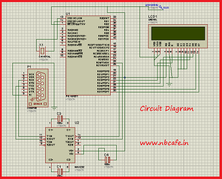
4. An ability to display information to the user via an LCD display.
5. An ability to identify an RFID tag using an RFID reader.

February 1, 2012 (5 hours):
Completed Introduction and Design Requirement sections of the Design Constraint Analysis Homework. For more details see the “Homeworks” section of the website.

February 2, 2012 (5 hours):
Completed Component Selection Rationale and Conclusion of Design Constraint Analysis Homework, as well as the initial parts list and revised block diagram. Finalized entire Design Contraint homework. Called up Microchip to obtain samples of the PIC24FJ256GA106 microcontroller. The samples should arrive late next week.

WEEK 04 SUMMARY
Accomplishments: Completed Design Contraint homework assignment. Finalized and ordered the microcontroller chosen for this project (PIC24FJ256GA106).
Weekly Work Total: 16 hours
Project Work Total: 42 hours

Week 05

February 8, 2012 (2 hours):
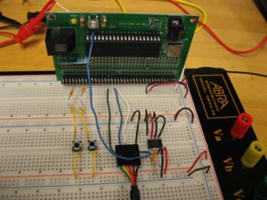
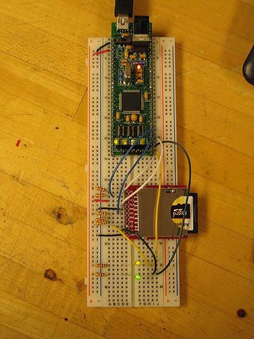
Met with Chuck to discuss debugging/testing methods for the PIC24FJ256GA106. Chuck supplied the group with an Explorer 16 development board for PIC24 microcontrollers, complete with a PIC24FJ128GA010 for development purposes. Installed the Microchip MPLAB IDE for use with PIC24 software development and testing, and downloaded the Microchip Memory Disk Drive File System Library for use with interfacing PIC micros to SD cards. Completed a demo tutorial on how to create a new MPLAB project, connect to the development board, download code, and debug the project on the microcontroller.

February 10, 2012 (3 hours):
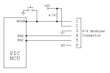
Continued to experiment with the Microchip MPLAB IDE that will be used as the development environment for the PIC24 microcontroller. Began to look at the datasheet for the PIC24FJ256GA106 to identify critical pins for initial programming, debugging, and functionality. For communication with the ICD 2 Debugger, connections must be made from the debugger to the MCLR (Master Clear) pin, PGEC/PGED pair, and Vcc/Vss. Also, due to the limited number of pins on the chosen microcontroller, pins for UART and SPI communication need to be assigned funcationality using the Peripheral Pin Select Registers. It seems as though the user is able to assign input and output pins to a given peripheral without much constraint, which will provide a large amount of freedom when designing the system. The PIC24FJ256GA106 micros that were ordered last week came in today, and the team talked with Chuck to place an order for microcontroller breakout boards to be used during initial experimenting and testing stages.

WEEK 05 SUMMARY
Accomplishments: Obtained the main microcontroller to be used for this project. Installed the IDE to be used with the PIC24 micro, and completed initial tutorials related to creating and building new projects. Began to look at critical pins on micro for initial programming and testing.
Weekly Work Total: 5 hours
Project Work Total: 47 hours

Week 06

February 14, 2012 (3 hours):
Researched and confirmed how several of the chosen peripherals for this project will interface with the PIC24FJ256GA106. Since the RFID unit operates on 5V, it was initally thought that level translators would be needed so that the 5V TTL serial logic could communicate with the 3.3V micro. After further research, it was discovered that the PIC24 device has several digital input pins that are tolerant up to 5.5V. This alleviates the need for any level translators between the two devices. Also, since the digitial compass I2C lines typically operate on 1.8V digital logic, it was confirmed that the Sparkfun breakout board has built-in level translators to ensure correct operation with the 3.3V micro. Lastly, it was discovered that only one of the PGECx/PGEDx pin pairs on the micro need to be connected to the ICD 2 debugging unit, and that the Configuration Bits (set in software) identify which pair is to be used.

February 15, 2012 (3 hours):
Soldered headers to the breakout board which Jeff previously soldered one of the PIC24 micros to. Verified connectivity for each of the pins on the breakout board, and used masking tape to label the microcontroller pin numbers. Began to add .1 uF decoupling capacitors to each Vdd/Vss pair, as well as the appropriate resistors for the MCLR pin as specified by the PIC24FJ246GA106 datasheet.

February 16, 2012 (5 hours):
Obtained the 10uF capacitor needed for the Vcap/Vddcore pin to allow the internal voltage regulator on the micro to convert the 3.3V Vdd to 2.5V for the microcontroller core. Obtained an RJ-11 cable from Chuck for use with the ICD 2 debugger, stripped the wires on one end, and soldered headers to the wires for use with the microcontroller breakout board. Applied initial power to the microcontroller breakout board, and was able to successfully connect to and program the micro via the MPLAB software. Created an initial hearbeat program using one of the timer modules and an interrupt, which toggles an I/O pin when the timer count reaches 0xFFFF. Since the peripheral clock for the microcontroller currently operates at 4MHz, the square wave generated should have a frequency of 4M / 2^16 / 2 ~= 30.5 Hz This result was successfully observed on an oscilloscope,

February 18, 2012 (2 hours):
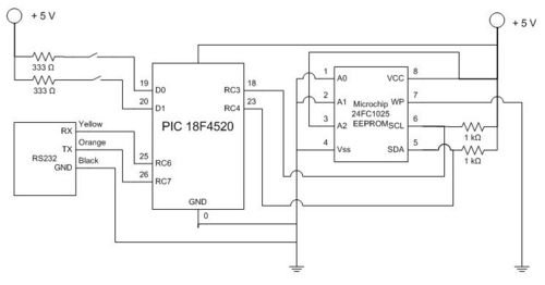
Met with Jeff to begin testing the newly obtained FT232 breakout board from Sparkfun. The goal for tonight was to be able transmit a single character from one of the UART modules on the microcontroller to the FT232, which would then transmit the character via USB to a virtual COM port on a PC. Initialized the UART1 module to 9600 baud, 8 bit data, no parity, and 1 stop bit. Placed a character in the UART1 transmit buffer, but was unable to retrieve the character on the PC side. Connected an oscilloscope to the Rx pin on the FT232, and could see that the character was correctly transmitted by the UART module, but would still not show up on the PC terminal.

WEEK 06 SUMMARY
Accomplishments: Verified how several peripherals would interface with the microcontroller. Successfully constructed a breakout board for the PIC24FJ256GA106, and created an initial “Hello World” heartbeat program to verify functionality. Began to interface with the FT232 module, but were unable to receive a character on the PC side.
Weekly Work Total: 13 hours
Project Work Total: 60 hours

Week 07

February 19, 2012 (3 hours):
Continued working on interfacing with the FT232 module, with the goal of receiving a character on the PC side sent from the UART1 module on the microcontroller. Soon found out that characters could be received on the PC via USB only when the power cord was connected to the laptop that was being used for communication. As soon as the power cord was removed, communication would stop. Began to look into USB power specs for laptop on battery vs. not on battery, but could not find any obvious solution to this strange problem. Wrote a basic function to transmit strings of data via UART, but soon found that the printf function in the library would automatically send data out via a properly initialized UART1 channel. This printf function will be very useful for debugging statements in the future.

February 20, 2012 (6 hours):
Fixed the problem with the FT232 only working when the power cord is attached to the laptop. Apparently, not all of the ground rails on the breadboard were connected together, and this was causing unpredictable behavior with the FT232 module. Began to create another test program using both the UART1 and UART2 modules of the microcontroller, with the goal of sending a character from the PC to the Rx pin of UART2 via the FT232 chip, then copying the character from the UART2 Rx buffer to the UART1 Tx buffer, and sending it back to the PC via UART1 and the FT232 chip. Ran into a whole bunch of weird issues, where only one UART module or the other would work at a time. After a lot of debugging, it was discovered that the Peripheral Pin Select registers, which controlled which pins were used for each peripheral module, were set by default to only allow one write sequence. Once this default setting was changed, both UART modules were able to work at the same time, and the echo to terminal program proved to be successful. Another program was also created to read in data from the RFID module via UART2, and verify the RFID code against a stored list of valid “keys”. This program also proved to be successful.

February 21, 2012 (8 hours):
Connected the GPS module to a breadboard and was able to recognize the device by using the Trimble GPS Studio PC program. Able to successfully configure the GPS device via the PC program, log messages, and convert the messages to ASCII text for further analysis. Unable to actually obtain any sort of GPS lock or coordinate data at this time due to lack of an antenna for the GPS device.

Moved focus from the GPS to the digital compass module, which interfaces via I2C. Researched the I2C protocol to understand the fundamental communication pattern between devices. Next, looked at the application notes and datasheet for the compass, to understand which registers to initialize for functionality. Began initializing the I2C1 module on the microcontroller for 100 KHz (standard mode), and creating routines to send and receive bytes to both the accelerometer (slave address 0x18) and the magnetometer (slave address 0x1E). After initializing I2C module and creating functions for communication, a test program was developed to retrieve accelerometer data and display it to the PC terminal. Programmed the micro and ran test code, but unable to retrieve data from the compass module. Placed a scope on the I2C lines, but did not see logic signals being transmitted. Further debugging will be necessary.

February 22, 2012 (3 hours):
Verified pins on microcontroller schematic to ensure correct PCB connections. Only the I2C lines and all Vcc/Vdd pins are required to be connected to very specific pins. All UART and SPI pins can be assigned to any RPx pin (reprogrammable peripheral pins) on the device, and any GPIO pins can be assigned to any Ryx pin, where ‘y’ is an I/O port letter, and ‘x’ is a corresponding pin number for that port.

February 23, 2012 (4 hours):
Focused on the compass and I2C module again. Suprisingly, after reconnecting the compass module to the micro, the I2C module worked immediately. Created a test program to obtain both accelerometer and magnetometer data, and display to the PC terminal (picture below). Partway through the night, the I2C stopped working and began displaying behavior similar to what was seen on Tuesday. After some tinkering with wires and reprogramming the micro, the module began working again with no actual changes in software. Could not replicate the problem again for the rest of the night. Not sure if this is a software or hardware problem yet, but leaning towards the hardware side.

WEEK 07 SUMMARY
Accomplishments: Able to communicate with PC via UART1 module, and RFID via UART2 module. Able to communicate with GPS via PC application. Able to obtain accelerometer and magnetometer data via I2C1 module, but errors may still exist either in hardware or software.
Weekly Work Total: 24 hours
Project Work Total: 84 hours

Week 08

February 27, 2012 (3 hours):
Shifted focus from software development to preparation for the upcoming Design Review on Wednesday. Created two powerpoint slides related to the preliminary software design and development status. Some of the software accomplishments thus far involve communicating with the FT232 module via UART1, receiving RFID data via UART2, and communication with the compass module via I2C. The next goals on the software side of things are initilizing communication with the GPS module (UART3), LCD screen (GPIO), and MicroSD card (SPI). Also created a small table catagorizing the pins used on the microcontroller into pins used for initial setup (Vcc/Vss/Debug/MCLR), pins used for serial communication (UART, SPI, I2C), GPIO pins for the LCD and pushbutton, and PWM pins for the speaker and servo. As of now, 13 pins are used for initial setup, 13 for serial communication, 15 for GPIO, and 2 for PWM. Altogether 43 of the 64 pins are currently in use. Began working on Component Selection slides, which will be heavily based off of the ones used for the Design Constraint presentation.

Joshua Marchi's Lab NotebookFebruary 28, 2012 (4 hours):
Completed the Component Selection slides for the Design Review tomorrow. The major component choices that will be discussed include the PIC24FJ256GA106 microcontroller, Trimble Copernicus II GPS Receiver, LSM303DLH Digital Compass, and ID-12 RFID receiver. Updated the block diagram for the project, removing the LEDs for user interface, and added the MAX17043 Fuel Gauge to monitor battery status. The LEDs were removed as the team believes the compass heading would be able to be displayed using the LCD screen instead, which would simplify the PCB design and also help to reduce power consumption for the project. Worked with Jeff to finish up the Schematic and Theory of Operation slides, and polished up the entire Powerpoint document for the presentation tomorrow.

March 3, 2012 (2 hours):
Worked with Jeff to re-connect the GPS module to the Trimble GPS application on the PC. The FT232 breakout board is used to provide a serial to USB conversion, so that the device can be recognized through a virtual COM port on the PC. Connected the newly obtained antenna to the GPS and applied power. The PC application was able to show the connection status of each satellite detected, and by moving the antenna to a window, enough satellites were discovered to start obtaining position data. The next step was to take the GPS unit (complete with breadboard) outdoors and test tracking while moving. The GPS was placed inside of the Pelican case, and the lid was placed on top to simulate normal operation. A route was walked, and then promptly repeated, since both teammates forgot to enable logging of data on the PC the first time. The data results were highly accurate, as shown in the image below (The team attempted to spell out “HI” near the bell tower), but the GPS had some problems initially discovering the satellites in between the first and second runs. More experimentation is required to determine if this was related to the positioning of the GPS, or some other factor.

WEEK 08 SUMMARY
Accomplishments: Prepared all required materials for the Design Review presentation, and performed initial satellite acquisition of the GPS module, in addition to logging and mapping data via the Trimble PC application
Weekly Work Total: 9 hours
Project Work Total: 93 hours

Week 09

March 4, 2012 (3 hours):
Created a detailed Excel document regarding pin assignments for the PIC24FJ256GA106. This spreadsheet includes a list of all pin numbers, all possible uses for each pin, whether or not the pin is 5V input tolerant, the chosen functionality of each pin for this project, the associated peripheral for each pin, and any special notes for each pin. This will help greatly in the upcoming week, since the pin assignments will most likely need to be shifted around before the PCB is finalized. Discussed proposed changes to the PCB with the rest of the team. Most likely, the GPIO pins for the LCD will be moved so that all of them correspond to pins on Port B, rather than scattered around Ports G, B, and F. Also, headers and traces might be added to the PCB to allow the second serial port on the GPS to be used in combination with an additional (removable) FT232 module for easy programming, logging, and mapping of GPS data for debugging purposes, even when connected to the PCB.

For more detail: Joshua Marchi’s Lab Notebook

The post Joshua Marchi’s Lab Notebook using pic microcontoller appeared first on PIC Microcontroller.

USB Keypad Demonstration – Crystal Free USB and mTouch™ Sensing Solutions using pic microcontoller

$
0
0

The USB keypad reference design demonstrates crystal free USB operation. Microchip has partnered with Lumvatech to demonstrate a low-cost aesthetic design, with touch capability and LED lighting integrated. All features are driven with a single PIC16F1459 MCU.

USB Keypad Demonstration - Crystal Free USB and mTouch™ Sensing SolutionsUSB is one of the most common serial interfaces used in a wide variety of applications. The USB 2.0 module with clock recovery from USB host, eliminates the need of an external crystal and thereby saving BOM costs and space on designs. The PIC16F145X family and PIC18FXXK50 families feature Active Clock Tuning which guarantees 0.25% accurate 48Mhz internal oscillator across all temperature range when connected to USB host.

This design also features the integration of 18 touch buttons based on the Capacitive Voltage Divider (CVD) technique from Microchip. A matrix-based approach is followed where of the 9 ADC channels available, five are used for row detection and four for column detection. Two columns are also used for proximity detection. LED backlight for the keypad with auto power off and audio feedback using the piezo buzzer is also implemented.

The USB keypad reference design demonstrates crystal free USB operation. Microchip has partnered with Lumvatech to demonstrate a low-cost aesthetic design, with touch capability and LED lighting integrated. All features are driven with a single PIC16F1459 MCU.

USB Keypad Demonstration - Crystal Free USB and mTouch™ Sensing SolutionsUSB is one of the most common serial interfaces used in a wide variety of applications. The USB 2.0 module with clock recovery from USB host, eliminates the need of an external crystal and thereby saving BOM costs and space on designs. The PIC16F145X family and PIC18FXXK50 families feature Active Clock Tuning which guarantees 0.25% accurate 48Mhz internal oscillator across all temperature range when connected to USB host.


For more detail: USB Keypad Demonstration – Crystal Free USB and mTouch™ Sensing Solutions

The post USB Keypad Demonstration – Crystal Free USB and mTouch™ Sensing Solutions using pic microcontoller appeared first on PIC Microcontroller.

PIC MCUs: Hardware and Connections using pic-microcontroller

$
0
0

Required Hardware

In order to program and debug a PIC microcontroller, you will need a few pieces of hardware.

PIC MCUs

ICD-U40

The ICD-U40 is an In-Circuit-Debugger/Programmer that allows the user, through CCS C Windows IDE, to program and interactively debug a PIC microcontroller.

5V DC Power Supply

Although the 4520 board has a voltage regulator that is capable of handling larger voltages (up to 30 volts), a five volt power supply should be used if available to avoid needing a heat sink for the regulator.

Hardware Connection

USB to ICD-U40

The first time the ICD-U40 is connected to a computer via a USB cable, a driver for the ICD-U40 needs to be installed. This driver can be found either on the installation disk that came with the CCS C Windows IDE, or on the CCS Inc. website: http://www.ccsinfo.com/content.php?page=ICD

ICD-U40 to PIC MCU

The ICD-U40 programmer/debugger connects to the PIC microcontroller through a six wire modular cable. Although the 4520 board is already wired correctly, a wiring diagram for communication with the PIC microcontroller is given below for reference.

While the ICD is connected to the PIC MCU and to your computer via a USB cable, the Windows IDE will be able to communicate with the PIC microcontroller. In order to program or debug successfully, these connections must be made correctly. Once all connections are made successfully the LED on the ICD-U40 will turn on.

PIC MCUs

PIC MCU Power

In order for all hardware conections to be successful, the PIC microcontroller unit itself must be powered. To do this, simply connect the pins of the MCU to power/ground as shown on the devices datasheet, or if you are using the 4520 board plug the five volt power supply into the barrel connector on the board. Also, ensure that all connections between the MCU and the ICD are made correctly as in the diagram above.


For more detail: PIC MCUs: Hardware and Connections

The post PIC MCUs: Hardware and Connections using pic-microcontroller appeared first on PIC Microcontroller.

Data logging with an EEPROM

$
0
0

Contents

   1 Original Assignment

Data logging with an EEPROMOriginal Assignment

Your task is to use the PIC to log data from an analog input on an EEPROM, and after the data collection is over, to send the data back from the EEPROM to a PC running matlab. Use an interrupt service routine to read an analog input and write the value to an external EEPROM using I2C. After reading in a fixed number of samples, perhaps 1,000 or 10,000, the program should send the data back to a matlab program via an RS-232 link. The logged data should then be plotted by matlab.

You should decrease the sample time until the ISR does not successfully complete. What is the fastest rate at which an analog input can be read and stored to the external EEPROM? Try this for an analog input configured for both 8-bit (1 byte of data stored on the EEPROM) and 10-bit (2 bytes of data stored on the EEPROM). How much data can you store on the EEPROM?

As an alternative, you can avoid the use of an ISR and simply read and store the data as fast as you can in a loop.

As a test input, use a triangle wave signal from the function generator between 1 and 4 V, and plot the data in matlab.

See Interfacing to External EEPROM, PIC RS232, and Serial communication with Matlab.

Overview

An external EEPROM is useful when trying to store data. In addition to storing much more data than is available on the 18F4520 PIC, an EEPROM stores the data even when power is removed and can then be collected at a later time. Storing large amounts of data over time is especially beneficial once communication can be made between the PIC and Matlab. Using the serial function in Matlab, the data can be obtained and then analyzed.
In this project, we used the PIC to log data from an analog input onto an EEPROM and then later sent the data back from the EEPROM to Matlab to plot. For our lab, we worked with a 24FC1025 EEPROM whose data sheet can be found here. Additionally, we established serial port connection between the PIC microcontroller and Matlab using the RS232. Our project also made use of two buttons. The first button tells the PIC to begin collecting data points from the analog input and storing the data onto the EEPROM. The second button tells the PIC to send the data from the EEPROM to Matlab.

Data logging with an EEPROMCircuit

To the right is a circuit diagram for interfacing a 24FC1025 EEPROM to the 18F4520 PIC. Below the diagram are photos of the circuit layout.
inputs on the PIC which dictate when to collect and store data and when to send the data to Matlab.


For more detail: Data logging with an EEPROM

The post Data logging with an EEPROM appeared first on PIC Microcontroller.

Analog Experiments Anywhere

$
0
0

Two DIY micro-controller based USB connected electronic units which along with the Texas Instruments Analog System Lab Starter kit and a laptop permit you to conduct analog experiments anywhere.

It would be wonderful  if senior students and laboratory supervisors built these units so that they could be used in their laboratories by freshers.

Aj-SigGen-PS     http://ajoyraman.in/DDS_SigGen_PS.html

Aj-Simple-Scope      http://ajoyraman.in/USB_Simple_Oscilloscope.html

Analog System Lab Starter Kit ASLKv2010    http://www.uniti.in/teaching-material/analog-system-lab-starter-kitAnalog Experiments Anywhere

Step 1: Aj-SigGen-PS

This unit is designed to compliment the Aj-Simple-Scope and serve as a teaching aid for budding engineers, electronic enthusiasts and hobbyists.

This USB connected unit implements a microcontroller based DDS Signal Generator providing Sin and Triangular waveforms with adjustable magnitude and offset up to 50 kHz. TTL and 1 V square waves are simultaneously provided. Additionally ± 12V and a variable +2 to 7V output with a total capacity of  1W is provided to power external circuits under test.

Step 2: Block Schematic and Function Description of Signal Generator and Power Supply Unit

For ease of portability the unit is powered and controlled from the USB port of a PC.

Two PIC18F14K50 microcontrollers are used to provide the functionality of the unit.

The first PIC microcontroller implements the following functions:

• Communicates with the host PC for enumeration as a USB to UART device

• Sets up the unit as a 500mA device

• Switches on power to the DC-DC converter

• Provides the complimentary square wave drive to the DC-DC converter

• Acts as a USB communication interface to the second PIC

• Provides the Amplitude reference for DAC2

• Provides the digital word for DAC1 giving the offset value.

The second PIC microcontroller implements the remaining DDS functions

• Direct Digital Synthesis (DDS) signal generation

• Sin/ triangle word output to DAC2

• TTL and 1 V square reference output

The DC-DC converter is a driven 1W, 5V to ± 12V operating at 100 kHz. The +12 V output is fed to a linear regulator to provide a variable +2 to 7 V output controlled by a variable potentiometer.

The DC-DC converter provides full protection to the host PC USB port as its outputs are short circuit and current limit protected.

The circuit under test can be rigged up on a standard breadboard and powered from the power sockets provided. Analog Experiments Anywhere schematich

Step 3: Aj-Simple-Scope

This unit is designed to compliment the Aj-SigGen-PS and serve as a teaching aid for budding engineers, electronic enthusiasts and hobbyists.

This USB connected unit implements a microcontroller based 2-Channel Oscilloscope providing continuous sampling rates up to 100 ksps and 20 Msps using equivalent time sampling. Common DSO features such as spectrum analysis, waveform capture and data saving are provided. The input range is ± 12V with additional gain settings of X2 and X5. Trigger and sweep options are also provided.


For more detail: Analog Experiments Anywhere

The post Analog Experiments Anywhere appeared first on PIC Microcontroller.

DS18S20 interfacing with pic and avr microcontroller

$
0
0

In this article you will learn how to interface temperature sensor DS18S20 with PIC16F877A microcontroller and atmega88 avr microcontroller. Complete interfacing circuit diagram and code for both PIC microcntroller and AVR microcontroller. DS18S20 interfacing with pic code is written using Mikro C for pic. Code for AVR microcontroller is written using Mikro basic complier for avr. Let’s start with basic introduction of DS18S20 digital thermometer.DS18S20 interfacing with pic and avr microcontroller

DS18S20 digital thermometer

DS18S20 is  9- bit digital thermometer which is used to measure celsius tempertaure. DS18S20 also have fuction of alaram with non-volatile user programmed points. It communicates with microcontrollers with only one wire. So it works with one wire communication protocol. It requires only one data line for communication. It can also be powered from data line. It remove the need of external power supply. Each DS18S20 have unique 32 bit address. Therefore it is  easy to interface multiple DS18S20’s with microcontroller.

DS18S20 applications

It have many applications. Some major applications are given below.

  • industrial temperature controller
  • buildings temperature controller
  • digital thermometers

DS18S20  features

It have following major features as compared to other digital thermometers:

  • one wire interfacing with microcontroller i.e. only one wire is required for data
  • alarm setting if temperature is outside permissible limits
  • Multiple devices can be interfaced with same microcotroller due to unique 64 bit address
  • Maximum accuracy
  • It can read temperature from -55°C to +125°C
  • No need of external components. It is ready to use by interfacing with microcontroller

DS18S20 pin configuration

It is available in 3 pin TO-92 package and 8 pin SO package

We are using 3 pin ds18s20 package in this tutorial.  Brief description of all the pins is given below:

  1. Number 1 : ground pin
  2. number 2: Data input and output pin. It is open drain one wire interfaced pin. It is also used for powered DS18S20.
  3. number 3:  5 volt power supply if not used in parasite power mode. if parasite power mode is used, it must be groundedDS18S20 interfacing with pic and avr microcontroller schematich

DS18s20 interfacing with PIC16F877A microcontroller

Circuit diagram for interfacing of DS18S20 is shown below. It is not used in parasite power mode. Therefore 5 volt power is connected externally.  DS18S20 is interfaced with pin zero of port D. PORT D pin zero is used for one wire communication with digital thermometer.  16 ×2 LCD is used to display temperature. LCD interfacing with pic microcontroller is used to display temperature.

DS18S20 interfacing with pic code

Code for this project is written using Mikro C pro for pic.


For more detail: DS18S20 interfacing with pic and avr microcontroller

The post DS18S20 interfacing with pic and avr microcontroller appeared first on PIC Microcontroller.

My New MIDI Merger uses 10 MIPS £1.00 PIC Microcontroller using PIC18F4320

$
0
0

This unit provides 4 autonomous MIDI inputs and 1 MIDI output. Note this is a ‘proper’ MIDI Merger – all 4 MIDI inputs can be used at the same time, unlike other ‘designs’. The unit also provides an indication of the channel number being played, and has shown itself to be capable of expansion into a full-blown controller.
The PIC microcontroller I used – 18F4320 was being sold off cheap, at £1.00 each by Crownhill Associates, in Ely – but don’t pester them for any 18F4320’s at this give-away price, as I bought the rest of their stock!
It’s always worthwhile to take a glance at their website, as inevitably they have PICs at discounts you wouldn’t find anywhere else. A purchase I made this week, was 5 PIC18F6620s – a 64-pin TQFP monster PIC – at only £2.00 per pop!

MIDI Merge

The intention here is to provide details of the schematic and photographs/advice on construction. The PIC code will be discussed more fully on http://picprojects.info.(shortly) All source-code is provided in this post, together with Eagle project files for the printed circuit boards.

The schematic is below. Apart from the PIC and it’s crystal, the other main components are 4 6N138 opto-isolators, 5 on-board DIN sockets, a voltage regulator, and a few resistors. I mounted the LEDs on a separate interface/indicator board, and the schematic for this is shown later. The handful of pin headers are used to add a key matrix and FTDI USB-TTL lead, for upgrading the software, using an internal bootloader.

Following are some views of the PCB. Note these are not all to the same scale. The complete Eagle project for the PCB is available for download.

As shown in the main schematic, the unit functions as a MIDI-Merger and Indicator. With the addition of a keypad, extensions to this are easily added. I added the following, mainly because I find them useful.

  • MIDI Minimum volume (set on a channel-by-channel basis)
  • MIDI Channel re-assign – Re-assign any MIDI Channel to another
  • Filter-out unwanted MIDI commands – Get rid of those pesky pitch-wheel messages from your MIDI Guitar Unit!

The front panel I have shown above – I created a separate user-interface board that incorporated a 16-key matrix, and duplicated the reset switch and LEDs.
The 4 resistors are 10K in value and the capacitor is 100nF. I used small TACT switches and extra-bright 3mm LED’s. I used 2- double-row pin headers to connect everything to the main board.


For more detail: My New MIDI Merger uses 10 MIPS £1.00 PIC Microcontroller using PIC18F4320

The post My New MIDI Merger uses 10 MIPS £1.00 PIC Microcontroller using PIC18F4320 appeared first on PIC Microcontroller.


PIC32MX: Interfacing to a Secure Digital (SD) Flash Card

$
0
0

Original Assignment

Do not erase this section!

Your assignment is to create code that will allow the PIC32 to read and write data to a FAT32 SD card. The SD card should be able to be read by a PC after data has been written on it by the PIC32.

Create functions so that it is easy to read, write and initialize the SD card.

Use the example projects in the “Microchip Solutions/USB Device – Mass Storage – SD card data logger” and “Microchip Solutions/USB Device – Mass Storage – SD card reader” folders as a guide.

Use your code to create a folder on the PIC32 and write 1000 bytes of data to a text file in that folder. How long does it take? Make sure the PC can read the file.

Interfacing to a Secure Digital (SD) Flash Card

Create a folder on the SD card with the PC and place a text file in the folder with 1000 bytes of data. Read the file with the PIC32. How long does it take?

Overview

Secure digital cards, or SD cards, are inexpensive and common mass storage devices that can be interfaced with our PIC to provide a larger non-volatile data storage space. Non-volatile memory is computer memory that retains information even when not powered. In this lab, we interfaced our PIC32MX460F512L to communicate with a 2GB FAT32 SD card to allow reading and writing of data.

The original program stems from tutorials from the book Programming 32-bit Microcontrollers in C: Exploring the PIC32 by Lucio Di Jasio. We used the tutorials from Day 14 and 15 to generate our code for SD card reading and writing via SPI communication (Serial Peripheral Interface). The main problem with this tutorial is that it is made for the PIC32MX360F512L on the Explorer16 board, so many changes were required in order to run the code.

NOTE: While ultimately, we were able to initialize the SD card and send data along the output and input lines, we were unsuccessful in executing the read/write demo. We are confident that the hardware configuration and circuit are correct, however the code likely contains errors.

Circuit

The SD card holder has 11 pins, 6 of which are being directly used for communication with our PIC. The SD card is powered off of 3.3V from our PIC, which comes from our mini-usb connection. 10K and 1K resistors pull-up resistors were added to each connection in order to allow for a voltage drop. Green and yellow LEDs were added to the Write Protect (WP) and Card Detect (CD) lines for ease of use. A powered yellow LED indicates the presence of an SD card in the SD card reader. A powered green LED indicates that the Write Protect is off. No resistor is necessary on the clock line. The IRQ and P9 pins on the SD card holder were not needed for SPI communication, so they were not connected to the PIC. However, they need to be powered for the SD card holder to operate properly. A breakdown of each of the 11 pins on the SD card holder is displayed in the table below.

NOTE: While ultimately, we were able to initialize the SD card and send data along the output and input lines, we were unsuccessful in executing the read/write demo. We are confident that the hardware configuration and circuit are correct, however the code likely contains errors.

Interfacing to a Secure Digital (SD) Flash Card

Circuit

The SD card holder has 11 pins, 6 of which are being directly used for communication with our PIC. The SD card is powered off of 3.3V from our PIC, which comes from our mini-usb connection. 10K and 1K resistors pull-up resistors were added to each connection in order to allow for a voltage drop. Green and yellow LEDs were added to the Write Protect (WP) and Card Detect (CD) lines for ease of use. A powered yellow LED indicates the presence of an SD card in the SD card reader. A powered green LED indicates that the Write Protect is off. No resistor is necessary on the clock line. The IRQ and P9 pins on the SD card holder were not needed for SPI communication, so they were not connected to the PIC. However, they need to be powered for the SD card holder to operate properly. A breakdown of each of the 11 pins on the SD card holder is displayed in the table below.

NOTE: While ultimately, we were able to initialize the SD card and send data along the output and input lines, we were unsuccessful in executing the read/write demo. We are confident that the hardware configuration and circuit are correct, however the code likely contains errors.


For more detail: PIC32MX: Interfacing to a Secure Digital (SD) Flash Card

The post PIC32MX: Interfacing to a Secure Digital (SD) Flash Card appeared first on PIC Microcontroller.

TTL to RS232 Signal Conversion

$
0
0

Methods:

  • Use a TTL HI output for the RS232 GND: Steve Walz of armory.com says “Use a TTL HI output for the RS232 *GROUND*!! Then you get +/-5VDC levels to fake out the RS232. When TTL-GND goes HI, then a TTL-XMT LO looks like -5VDC and a “mark”. Even sign problems go away in hardware! When TTL-GND goes LO, and TTL-XMT goes HI, it looks like +5VDC and a “space”! You can derive the two TTL signals from one off an inverter or inverter pair! Then magically, you have direct TTL to RS232 conversion!!

TTL to RS232 Signal Conversion

M. Adam Davis points out that we should “Just *make sure* the power supply of the pic and/or the power supply of the other rs-232 device are not grounded. ie, my bench power supply has +5v and ground, but the ground is grounded to the house ground, SO is the computer’s rs-232 port. I can’t use this trick without isolation. This also means that any interaction with other external devices requires some thoughtful planning.” [Ed: this is only true if the devices confuse signal ground and chassis ground. Remember that ground is at DB25 pin 7, and not pin 1 Pin 1 is chassis ground, not signal ground.]

Bob Ammerman [RAMMERMAN at PRODIGY.NET] of RAm Systems says:

Here is a neat trick to get a ‘push-pull’ output from two PORT A pins:1: define them as analog (ADCON1)
2: TRIS them as outputs.

Now, when you BSF either of them the other will automatically be cleared.

Andrew Warren says:

Of course, if you can’t configure the pins as analog inputs (because, for instance, the PIC you’re using doesn’t HAVE an A/D converter), you can do this:

        MOVLW   00000001B       ;RA0 = 1, RA1 = 0.
        MOVWF   PORTA           ;

        MOVLW   00000011B
        XORWF   PORTA           ;Toggle RA0 and RA1.
        XORWF   PORTA           ;Toggle the two pins again.
        XORWF   PORTA           ;And again...

Or, if those two pins are the only ones defined as outputs on that port:

        MOVLW   00000001B       ;RA0 = 1, RA1 = 0.
        MOVWF   PORTA           ;

        COMF    PORTA           ;Toggle RA0 and RA1.
        COMF    PORTA           ;Again.
        COMF    PORTA           ;And again...


TTL to RS232 Signal Conversion Schemetic


For more detail: TTL to RS232 Signal Conversion

The post TTL to RS232 Signal Conversion appeared first on PIC Microcontroller.

PIC12F675 Comparator Code and Proteus Simulation

$
0
0

This post provides the comparator code for PIC12F675 microcontroller. As we know, PIC12F675 microcontroller has one built in op-amp, which can be used as comparator. This code is written in C language using MPLAB with HI-TECH C compiler. You can download this code from the ‘Downloads‘ section at the bottom of this page.

PIC12F675 Comparator

It is assumed that you know how to blink an LED with PIC12F675 microcontroller. If you don’t then please read this page first, before proceeding with this article.

The result of simulating the code in Proteus is shown below[1].

In the above circuit[2], a variable voltage signal of 0 to 5 volts can be applied on Pin6 of PIC12F675 controller. Pin7 and Pin6 are the input pins for the comparator and Pin5 is output pin. In the above circuit shown, Pin6 is attached with the -ve pin of the comparator and on the +ve pin a reference voltage of 2.5v are applied internally. LED attached on the GP5 pin shows the result of the comparator.

So, in the above figure, GP5 pin is high because voltage on Pin6 of PIC12F675 is 2.45v, which is less than 2.5v. If a voltage higher than 2.5v is applied on Pin6, then GP5 will become low.

PIC12F675 Comparator schematic

Code

The code for the main function is shown below.

Downloads

Comparator code for PIC12F675 was compiled in MPLAB v8.85 with HI-TECH C v9.83 compiler and simulation was made in Proteus v7.10. To download code and Proteus simulation click here.


For more detail: PIC12F675 Comparator Code and Proteus Simulation

The post PIC12F675 Comparator Code and Proteus Simulation appeared first on PIC Microcontroller.

Serial communication with Pic 16f877 using UART

$
0
0

Abstract of that project: Using UART port we can establish serial communication between any devices. Here in my project Serial communication with Pic 16f877 using UART I will show you how easily we establish communication between two devices. In my project we know the pin no 25,26 in PIC16F877 are use as UART. The pin number 25 is use for receiving and 26 is used for transmitting.

Hardware needed: See the circuit diagram bellow we use MAX232,UART port, Pic16f877 and LCd (Lm106L) to make our project.

Serial communication with Pic 16f877 using UART circuit


For Simulation: we use Mikcro C pro to write the embedded C program for PIC16F877. We used Proteus 7 Professional for simulation. And for simulation of our project Serial communication with Pic 16f877 using UART, we replace COMPIM and MAX232 with Virtual UART Terminal.

So see our replace circuit for simulation in Proteus in bellow.

Serial communication with Pic 16f877 using UART schematic


Mikcro C Pro Code:

To interfacing UART with Pic we have to use some new command those are

UART1_Init(Baudrate):is Initialize UART module at specified baudrate.

 UART1_Data_Ready() : use to check data is receive or not.

 UART1_Write_Text(“Start”): use to write declared text on uart

 UART1_Write(): use for transmit uart data.

 UART1_Read(): use for read the uart data.

 Now see at below the programing code to understand use of above mention command.

For more detail: Serial communication with Pic 16f877 using UART

The post Serial communication with Pic 16f877 using UART appeared first on PIC Microcontroller.

10 tricks for interfacing to the PIC16C508

$
0
0

Most of the ideas in this chapter can be found on the pages of this website, but just in case you want to go over the capabilities of the ‘508A, we have brought them together.

Quite often when you are programming, the first thing you will run out of is output lines. Many projects need lots of drive lines and if you need more than about 8, you should go to another micro-controller.

Don’t expect an 8-pin chip to perform the impossible.

The designers of the ‘508A have done an amazing job providing 5 output lines (and one input line) in an 8-pin chip, but even so, many projects run out of drive-lines.

On other pages of this course we have shown how to expand the drive lines with a binary counter or shift register. This can increase the lines to more than 10 however if you want to add just one or two more devices than the chip is directly capable of handling (5), there are clever ways to connect them to the chip.10 tricks for interfacing to the PIC16C508

1. LED AND PIEZO ON ONE LINE

One of the simplest combinations is a LED and Piezo on a single drive-line as shown in fig: 1. These can be combined because the requirements of a LED are different to a piezo. A LED requires a constant HIGH for it to illuminate while a piezo requires a HIGH-LOW-HIGH waveform at approx 3kHz to produce a tone.

If the mark-space ratio of this waveform is kept short as shown in fig: 2, the LED will only illuminate very dimly. A short mark-space ratio means the “mark” is very small compared to the “space”. A very short on-time (mark) and a long off-time (space) will not affect the tone from the piezo but will deliver very little energy to the LED and this is exactly what we want.

On the other hand, each time the LED is activated, only a very small click will be heard, and this will hardly be noticeable. In this way the two devices can be combined on the same line.

2. LED AND PUSH BUTTON ON ONE LINE

In this book, we show how to connect two and up to five or more push buttons on a single input line and generally you will not have any problems adding buttons to a project. But if you want to add a secret reset button (or a “cheat” button, for example), it can be added across an existing LED as shown in fig: 3.

The resistor between the switch and micro acts as a safety resistor to prevent the output of the chip being damaged if the switch is pressed when the LED is activated, and it also acts as a dropper resistor for the LED.

These two items will work in combination because the impedance of the LED is very high when no voltage is across it and when the micro turns the line into an input line, it sees the LED as a high impedance. In other words it is not detected so that when the switch is pressed the micro only sees the switch as a LOW.

3. DIFFERENT PROGRAMS IN THE CHIP

Up to 5 different programs can be burnt into a single ‘508A and the required program can be accessed by soldering a resistor between one of the outputs and the “input-only” line – GP3, as shown in fig: 4.

During turn-on, a special program will put a HIGH on each output in turn and the output containing the resistor will determine the program.

Combining 5 programs in one chip will reduce inventory costs as the required program can be selected by fitting the resistor in the appropriate place on the board.

4. LINE REVERSAL

If a device is connected between two output lines as shown in fig: 5, a program can be written so that the device sees a voltage reversal. When one output is HIGH the other is LOW and this is then reversed.

The drive lines have a maximum output current of 25mA and this is enough to drive a number of different devices. If a red LED is connected in one direction and a green LED in the opposite direction, they can be turned on and off individually, as shown in fig: 6.

If the two LEDs are placed near each other or combined in the one LED (called a tri-coloured LED), they will produce a number of colours including orange, depending on the mark-space waveform delivered to each LED.

A single LED containing red and green chips is available in 2 or 3 lead versions. The wiring for a 3-leaded tri-colour LED is shown in fig: 7. The tri-leaded version is shown in fig: 6.

Tri-coloured LEDs are fairly expensive but if the project can cover the expense, they can be the basis of “running message” displays and simple TV screens.

If you connect a piezo to two out-of-phase lines as shown in fig: 8b, the sound produced will be slightly louder than the arrangement in fig: 8a.

When we talk about a piezo we really mean a PIEZO DIAPHRAGM. A piezo diaphragm is a passive device and is very similar to a capacitor as far as the circuit is concerned. Ceramic substrate on a metal diaphragm causes the metal to “dish” and bend to produce a high pitched sound. The size of the voltage (the amplitude) determines the intensity of the sound and the frequency of the waveform determines the tone.

The voltage across the piezo from one drive line is about 5v whereas the voltage seen by the piezo from two reversing lines is about 10v. Unfortunately this doesn’t produce twice the sound output but the sound is slightly louder. If you want a louder output you should use a better-quality high-output diaphragm (such as from a Christmas card).

The loudest output is a piezo siren and this is an active device containing a transistor oscillator and choke. These units operate from 5v to 15v and produce a very loud output while consuming only about 10mA to 15mA.10 tricks for interfacing to the PIC16C508 schematich

5. DRIVING LEDs

Each output line of a ‘508A can only deliver about 25mA. This current is determined by the size of the transistor delivering the current. The transistor inside the chip is only very tiny and if a higher current is drawn, it may be damaged.

When a resistance of 200 ohms is connected from output to ground, a current of 25mA flows (when the output is HIGH). If the resistance is reduced, a higher current flows. This means a resistance of 200 ohms or higher is required to make sure the current flow is less than 25mA.

But if a LED is placed on the output, how is the resistance worked out?

A LED drops a voltage across it according to its colour. This is called the CHARACTERISTIC voltage or the CHARACTERISTIC VOLTAGE DROP. This voltage is constant, no matter how bright the LED is illuminated.

For a red LED the characteristic voltage is 1.7v.

For an orange LED the characteristic voltage is 1.9v.

For a green LED the characteristic voltage is 2.1v.

LEDs cannot be connected directly to the output of a drive-line without a voltage-dropping resistor.

The reason is very technical but basically a red LED does not turn on AT ALL until exactly 1.7v is placed across it and if the voltage tries to rise above 1.7v, the LED will glow brighter, allow a very high current to flow and will be damaged.

The only way to prevent damaging the LED is to provide it with a very accurate supply voltage or simply connect a resistor in series. If the value of the resistance is worked out, an accurate current can be delivered to the LED and everything will be ok. The LED will last 100 years!


For more detail: 10 tricks for interfacing to the PIC16C508

The post 10 tricks for interfacing to the PIC16C508 appeared first on PIC Microcontroller.

Viewing all 320 articles
Browse latest View live


<script src="https://jsc.adskeeper.com/r/s/rssing.com.1596347.js" async> </script>